FYP Part A: MRI Reconstruction on FPGA Hardware - FPGA Architecture Overview
Here you will find the Cyclone V FPGA Architecture Overview in the interim report for my Final Year Project.
Other sections of the interim report may be put into their respective posts as individual research pieces. As part B of my FYP commences, I will be logging the progress and challenges that arise.
Chapter 3: FPGA Architecture
The following sections are based on the Cyclone® V Device Handbook [20].
3.1 Overview
At their core, FPGAs consist of configurable blocks of logic, known as Logic Array Blocks (LABs) in the context of the Intel® (previously Altera) Cyclone V GX FPGA used for this project. Each LAB contains Adaptive Logic Modules (ALMs) that can be configured to implement combinational logic, arithmetic, or memory operations. Separate from LABs are dedicated hardware resources designed to accelerate specific operations, including Digital Signal Processing (DSP) blocks and embedded memory blocks. Operations such as Fast Fourier Transforms (FFTs) and Finite Impulse Response (FIR) filters can be implemented using a combination of these specialised resources and ALMs, which are well suited to accelerating MRI reconstruction workloads. FPGAs contain multiple types of embedded memory resources, so care should be taken not to confuse Memory Logic Array Blocks (MLABs) which are built from ALMs inside of a LAB, with dedicated M10K memory resource blocks. A high-level overview of LAB structure with its interconnects is shown in Figure 3.1.
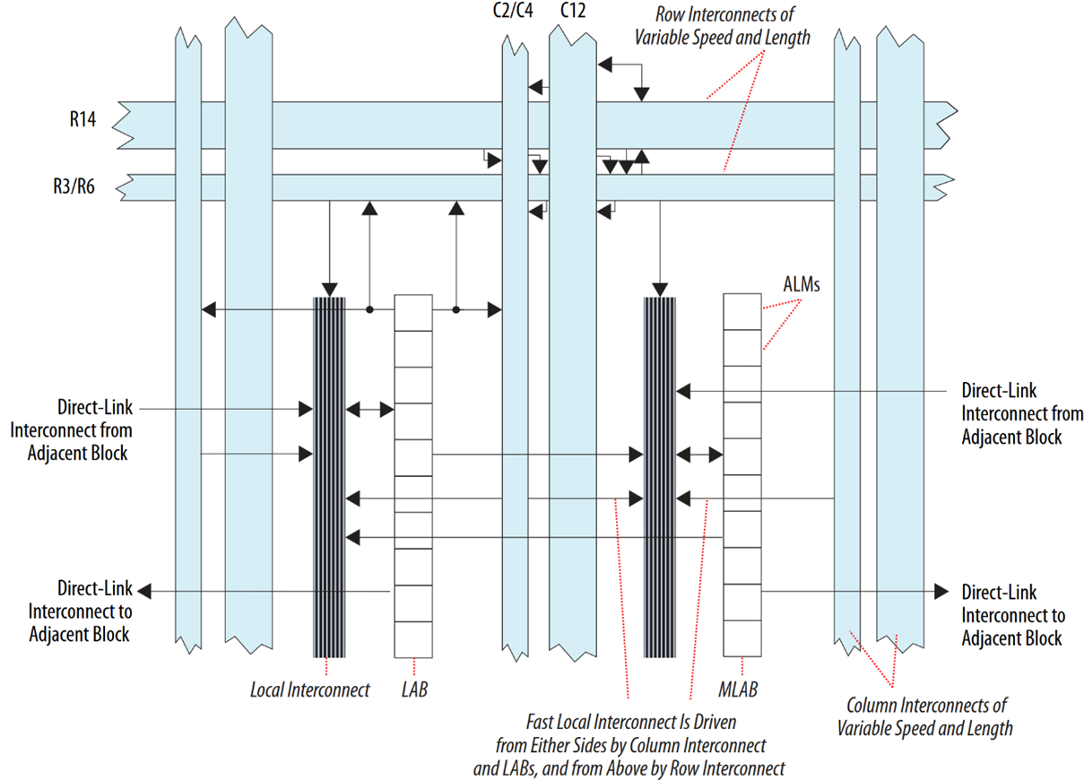 Figure 3.1: Structural Overview of LABs and Interconnects in Cyclone V FPGAs
Each ALM in a LAB contains four programmable registers, with each register containing a port for Data, Clock, Synchronous and Asynchronous Clear, and Synchronous Load. The Clock and Clear control signals of an ALM register can be driven by internal logic, general purpose I/O (GPIO), and global signals, while the Clock Enable (CE) signal is driven by GPIO pins or internal logic. In the case an ALM is used for combinational operations, the registers are bypassed and the output of the Lookup Table (LUT) directly drives the output of the ALM. A high-level block diagram of ALM architecture for Cyclone V FPGAs is shown in Figure 3.2.
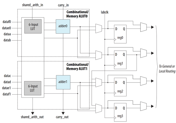 Figure 3.2: High-Level Overview of ALM Architecture in Cyclone V FPGAs
3.2 Interconnects
The Cyclone V family of FPGAs implements a hierarchical architecture for its interconnects, with each interconnect providing a different scope for routing and performance within the core.
3.2.1 Row / Column Interconnect
The row and column interconnect seen in blue in Figure 3.1 form the global, long distance routing network within the FPGA core. It spans across multiple LABs, MLABs, and memory and DSP blocks. These interconnects introduce higher latency compared to local and direct link interconnects due to length and routing complexity, but provide the most flexibility.
3.2.2 Local Interconnect
Local interconnects operate within a single LAB and are used to connect ALMs and other LAB-level resources such as LAB inputs, Lookup Table (LUT) outputs, and registers. The local interconnect allows each LAB to house ten ALMs.
3.2.3 Direct Link Interconnect
Direct link interconnects provide a path to connect adjacent LABs, MLABs, and memory and DSP blocks directly, without entering the row and column interconnect. To further minimise use of the slower row and column interconnects, each LAB and by extension MLABs, memory blocks and DSP blocks can also drive the LABs local interconnect using the direct link interconnect. This allows a single LAB to drive up to thirty total ALMs (ten ALMs internally, and ten in each adjacent LAB).
3.3 Memory Architecture
Like logic elements, the way memory is utilised for buffering and data storage on FPGAs is not fixed like in traditional CPUs and GPUs. Rather, the Cyclone V core provides on-chip memory through the M10K (10 kilo-bit embedded RAM) blocks with support for soft Error Correction (ECC) for general data storage, and then distributed memory through MLABs, enabling small memory structures close to the logic for low latency. However, only 25% of the available ALMs may be used to construct a MLAB.
The memory capacity of a MLAB is dependent on the amount of ALMs utilised. Consider that each ALM can be configured as a 32 x 2 bit memory block, then if all ten ALMs are configured this results in a 32 x 20 (640 bit) dual-port Static Random Access Memory (SRAM) block. This adaptability in local memory capacity and ALM utilisation allows for granular optimisation of each LAB for effective cache size versus logic density for a desired workload. Cyclone V FPGAs also support external Double Data Rate (DDR2, DDR3) and Low-Power DDR (LPDDR2) memory through dedicated memory controller blocks, allowing connection to off-chip SRAM and Dynamic RAM (DRAM), typically included on commercial development kits.
3.4 Lookup Tables (LUTs)
Each ALM contains a fracturable LUT structure that can be configured to implement either a single complex logic function, or multiple smaller functions, depending on resource requirements. They achieve this by storing the output values of a truth table in memory, rather than hardwiring physical logic gates. These LUTs are supported by the arithmetic circuitry and registers in an ALM as seen in Figure 3.2, allowing them to be combined with sequential elements to form complex logic structures such as shared arithmetic chains and carry propagation by utilising local and direct interconnects to minimise latency.
It is through LUTs and their small, integrated memory elements that ALMs can be configured as distributed memory to form an MLAB, allowing them to operate as SRAM blocks rather than purely combinational logic.
3.5 Intellectual Property (IP) Blocks
Intellectual Property (IP) blocks are pre-designed hardware modules supplied by the FPGA vendor (Altera, in this context) to implement complex functionality without requiring the user to develop complicated hardware descriptions. IP blocks may be classified as either Soft or Hard implementations. Soft IP blocks are implemented using a combination of ALMs, DSP blocks, and embedded memory resources. They are typically provided as a synthesizable hardware description allowing a high degree of flexibility in their configuration and implementation. However, this flexibility comes at the expense of logic utilisation, eating into the limited ALM, DSP, and memory resources. Hard IP blocks by contrast are implemented as fixed, dedicated silicon within the FPGA itself and do not utilise ALMs or DSP blocks for their intended functions, but are still able to interface with the FPGA interconnects allowing them to be integrated into most designs. Functionally, both soft and hard IP implementations can be seen as an abstraction layer above the base FPGA architecture for rapid development of complex components, hence why they are licensed and the intricacies of the designs and implementations are protected against theft and reverse engineering.
An example of hard IP on the Cyclone V GX FPGA is the implementation of PCIe 2.0 which integrates the Media Access Control (MAC), data link, and transaction layers within a single block, reducing logic utilisation and improving throughput compared to soft implementations.
3.6 Digital Signal Processing (DSP) Block
The DSP blocks inside of the Cyclone V core are dedicated hardware resources designed to implement complex arithmetic operations. They are variable precision, and support fully registered multiplication with 9-bit, 18-bit, and 27-bit word lengths for execution of arithmetic functions with reduced latency compared to implementations using general purpose logic or ALMs. Each DSP integrates multipliers, adders, and dual 64-bit accumulation units. The internal architecture makes use of pre-adders, a coefficient register bank, systolic registers, and register banks for input and output. This allows a DSP block to support multiply-accumulate operations with configuration into a dual 18 x 19 or single 27 x 27 multiplication unit, and systolic FIR filters with dedicated hardware for symmetric filter implementations. See Figure 3.3 for an overview of the DSP block architecture.
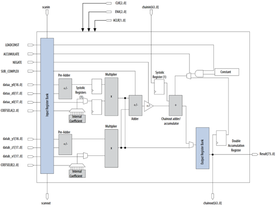 Figure 3.3: Variable Precision DSP Block Architecture for Cyclone V Devices
The internal structure of DSP blocks supports cascading between adjacent blocks through a 64-bit chainout adder that allows for propagation to adjacent DSP blocks without use of external logic or global interconnects, though they are also integrated with the interconnect network to enable data transfer between distant DSP blocks, embedded or external memory resources, and ALMs. Intel provides soft IP cores through the Intel Quartus Prime software to select different modes of operation for the DSP blocks, depending on the requirements of the design.
3.6.1 FFT and FIR Filtering in Hardware
Altera provides a high-performance soft IP core to implement a radix-2/4 decimation-in-frequency (DIF) FFT algorithm, internally using a block-floating-point (BFPU) architecture to maximise signal dynamic range in the transform calculation. Additionally, the FFT core can be configured for inverse FFT, and as a streaming FFT for continuous output data, suitable for progressive MRI reconstruction [18]. A block diagram of a single-output FFT implementation can be seen in Figure 3.4.
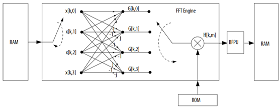 Figure 3.4: Block Diagram of a Single-Output FFT Soft IP Core
There is also an FIR soft IP core with support for single rate, decimation, interpolation, and fractional rate filtering, with configurable variable precision output [21]. A basic FIR filter structure with a weighted tapped delay line is shown in Figure 3.5.
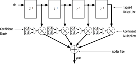 Figure 3.5: Block Diagram of a Basic FIR Filter with Weighted Tapped Delay Line
References
[18] Altera Corporation, “FFT IP Core - User Guide,” 2017. [Online]. Available: https://docs.altera.com/r/docs/683374/17.1/fft-ip-core-user-guide/fft-ip-core-functional-description.
[20] Intel Corporation (previously Altera Corporation), “Cyclone® V Device Handbook - Volume 1: Device Interfaces and Integration,” 2023. [Online]. Available: https://www.intel.com/programmable/technical-pdfs/683375.pdf.
[21] Altera Corporation, “FIR II IP Intel FPGA IP,” 17 September 2017. [Online]. Available: https://docs.altera.com/r/docs/683208/24.1/fir-ii-ip-intel-fpga-ip-user-guide/about-the-fir-ii-ip-intel-fpga-ip.